Physics classes by Nayan jha providing , The following case-study questions are based on important concepts of Semiconductor Electronics. These are useful for CBSE board examination preparation.
(Note- this is the proto type questions to practice the students preparing for board examinations.)
Case Study – 1: Based on the formation of PN Junction
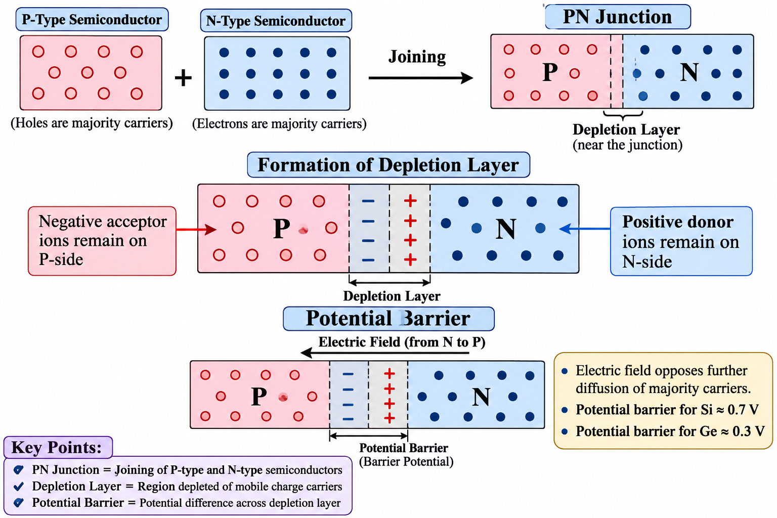
A PN junction is formed by joining a P-type semiconductor with an N-type semiconductor. When these two regions are joined, electrons from the N-region diffuse towards the P-region, while holes from the P-region diffuse towards the N-region. Near the junction, electrons and holes recombine, resulting in the formation of a depletion layer. Due to immobile ions, an electric field is developed across the depletion region, which produces a potential barrier.
Answer the following questions:
(a) What are the majority charge carriers in P-type and N-type semiconductors?
(i) Electrons and holes
(ii) Holes and electrons
(iii) Protons and electrons
(iv) Neutrons and holes
(b) The depletion layer is formed due to:
(i) Drift of electrons only
(ii) Recombination of electrons and holes
(iii) Movement of protons
(iv) Heating effect
(c) Which ions are present on the P-side of the depletion layer?
(i) Positive donor ions
(ii) Negative acceptor ions
(iii) Positive donor and negative donor ions
(iv) Neutral ions
(d) The potential barrier for a silicon PN junction is approximately:
(i) 0.1 V
(ii) 0.3 V
(iii) 0.7 V
(iv) 1.5 V
Case Study – 2: questions based on the forward and Reverse Biasing
A PN junction diode can be connected to an external battery in two ways: forward biasing and reverse biasing.
In forward biasing, the P-side is connected to the positive terminal and the N-side to the negative terminal of the battery. This reduces the depletion layer width and potential barrier, allowing current to flow easily.
In reverse biasing, the P-side is connected to the negative terminal and the N-side to the positive terminal. This increases the depletion layer width and potential barrier, resulting in a very small current.
Answer the following questions:
(a) In forward biasing, the P-side is connected to:
(i) Negative terminal
(ii) Positive terminal
(iii) Both terminals
(iv) Ground
(b) During forward biasing, the depletion layer width:
(i) Increases
(ii) Decreases
(iii) Remains constant
(iv) Becomes infinite
(c) During reverse biasing, the current through the diode is:
(i) Very large
(ii) Zero in all practical conditions
(iii) Very small
(iv) Infinite
(d) In reverse biasing, the potential barrier:
(i) Decreases
(ii) Increases
(iii) Becomes zero
(iv) Remains unchanged
Case Study – 3: Questions based on the semiconductor Diode as a Rectifier
A semiconductor diode is an important electronic device used for converting alternating current (AC) into direct current (DC). This process is called rectification.
A PN junction diode allows current to flow mainly in one direction. During the positive half-cycle of AC, the diode becomes forward biased and conducts current. During the negative half-cycle, it becomes reverse biased and does not conduct appreciable current.
Answer the following questions:
(a) The process of converting AC into DC is called:
(i) Amplification
(ii) Rectification
(iii) Modulation
(iv) Oscillation
(b) A PN junction diode allows current to flow mainly:
(i) In both directions equally
(ii) In one direction only
(iii) In no direction
(iv) Only in reverse bias
(c) During the positive half-cycle, a forward-biased diode:
(i) Does not conduct
(ii) Conducts current
(iii) Acts as an insulator
(iv) Breaks down
(d) Which device is commonly used for rectification?
(i) Transistor
(ii) Capacitor
(iii) PN junction diode
(iv) Resistor
Case Study – 4: Questions based on the Zener Diode****
A Zener diode is a specially designed semiconductor diode that operates in the reverse breakdown region. It is heavily doped and has a thin depletion layer. When the reverse voltage reaches a particular value called the Zener voltage, the diode starts conducting a large reverse current while maintaining an almost constant voltage across it. Therefore, it is commonly used as a voltage regulator.
Answer the following questions:
(a) A Zener diode is generally operated in:
(i) Forward bias
(ii) Reverse breakdown region
(iii) Zero bias
(iv) Forward breakdown region
(b) A Zener diode is mainly used as:
(i) Current amplifier
(ii) Voltage regulator
(iii) Rectifier only
(iv) Oscillator
(c) The depletion layer of a Zener diode is:
(i) Very thick
(ii) Very thin
(iii) Infinite
(iv) Absent
(d) The voltage across a Zener diode in its breakdown region is approximately:
(i) Zero
(ii) Constant
(iii) Continuously increasing
(iv) Infinite
Case Study – 5: Questions based on the Intrinsic and Extrinsic Semiconductors
Semiconductors are classified into intrinsic and extrinsic semiconductors. An intrinsic semiconductor is a pure semiconductor without any impurity. In an intrinsic semiconductor, the number of electrons is equal to the number of holes. When a small amount of impurity is added to a pure semiconductor, it becomes an extrinsic semiconductor. Depending upon the type of impurity added, it can be classified as P-type or N-type.
Answer the following questions:
(a) A pure semiconductor is called:
(i) Extrinsic semiconductor
(ii) Intrinsic semiconductor
(iii) Metallic conductor
(iv) Insulator
(b) In an intrinsic semiconductor, the number of electrons and holes is:
(i) Equal
(ii) Unequal
(iii) Zero
(iv) Infinite
(c) Which impurity is used to obtain an N-type semiconductor?
(i) Boron
(ii) Aluminium
(iii) Phosphorus
(iv) Gallium
(d) The majority charge carriers in a P-type semiconductor are:
(i) Electrons
(ii) Holes
(iii) Protons
(iv) Neutrons
Answer Key
| Case Study | (a) | (b) | (c) | (d) |
| 1. PN Junction | (ii) | (ii) | (ii) | (iii) |
| 2. Biasing | (ii) | (ii) | (iii) | (ii) |
| 3. Rectifier | (ii) | (ii) | (ii) | (iii) |
| 4. Zener Diode | (ii) | (ii) | (ii) | (ii) |
| 5. Semiconductors | (ii) | (i) | (iii) | (ii) |