PN Junction Diode, Depletion Layer and Potential Barrier
Class 12 Physics – CBSE Board Examination
1. What is a PN Junction?
A PN junction is formed when a P-type semiconductor is joined with an N-type semiconductor in such a way that a continuous crystal structure is formed.
P-type semiconductor: It is formed by doping a pure semiconductor (Si or Ge) with a trivalent impurity such as Boron or Alluminium. Holes are the majority charge carriers.
N-type semiconductor: It is formed by doping a pure semiconductor with a pentavalent impurity such as Phosphorus or Arsenic. Electrons are the majority charge carriers.
When these two types of semiconductors are joined, a PN junction is formed.
2. Formation of Depletion Layer
The formation of the depletion layer in a PN junction takes place due to the diffusion of charge carriers.
Step-by-step explanation:
step-1; When P-type and N-type semiconductors are joined, there is a difference in the concentration of charge carriers on both sides.
step-2; Due to this concentration difference, electrons from the N-region start moving towards the P-region, while holes from the P-region start moving towards the N-region.
step-3; Near the junction, electrons and holes recombine with each other.
step-4; As a result of recombination, the region near the junction becomes free from mobile charge carriers.
step-5; The N-side near the junction develops positively charged immobile donor ions, whereas the P-side develops negatively charged immobile acceptor ions.
step-6; Thus, a thin region is formed around the junction which is depleted of free electrons and holes.
This region is called the depletion layer or depletion region.
Definition for CBSE Examination:
The region around a PN junction which is depleted of free electrons and holes due to the recombination of charge carriers is called the depletion layer.
Diagram of depletion layer:
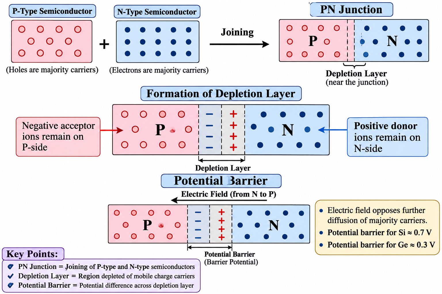
3. What is Potential Barrier?
During the formation of the depletion layer, immobile positive ions are left on the N-side and immobile negative ions are left on the P-side.
These charged ions create an electric field across the depletion region.
This electric field opposes the further diffusion of majority charge carriers across the junction.
As a result, a potential difference is developed across the depletion layer.
This potential difference is called the potential barrier or barrier potential.
Definition for CBSE Examination:
The potential difference developed across the depletion layer of a PN junction, which opposes the further diffusion of majority charge carriers, is called the potential barrier.
Value of Potential Barrier
At room temperature (approximately 300 K):
| Semiconductor | Potential Barrier |
| Silicon (Si) | 0.7 V |
| Germanium (Ge) | 0.3 V |
4. How is the Depletion Layer Formed? (Complete Explanation)
The formation of the depletion layer can be understood through the following process:
As we know The P-region contains a large number of holes and N-region contains a large number of free electrons. After joining themElectrons diffuse from the N-region to the P-region Holes diffuse from the P-region to the N-region. Then the Electrons and holes recombine near the junction the mobile charge carriers disappear from this region.This is the cause of formation of immobile ions in which ,Positive donor ions remain on the N-side negative acceptor ions remain on the P-side. Finally, An electric field develops across the depletion region. A potential barrier is established. This barrier opposes further diffusion of majority charge carriers.
At equilibrium, the diffusion current and drift current become equal and opposite. Therefore, the net current through the junction becomes zero when no external voltage is applied.
5. Difference Between Depletion Layer and Potential Barrier
| Depletion Layer | Potential Barrier |
| It is a region around the PN junction. | It is a potential difference across the depletion region. |
| It is formed due to recombination of electrons and holes. | It is developed due to immobile charged ions. |
| It contains immobile positive and negative ions. | It opposes the diffusion of majority charge carriers. |
| Its width can change with applied voltage. | Its value depends on the semiconductor material and applied conditions. |
6. Important Questions for CBSE Board Examination
Very Short Answer Questions (1 Mark)
- What is a PN junction?
- Define depletion layer.
- What is meant by potential barrier?
- What are the majority charge carriers in P-type and N-type semiconductors?
- What is the potential barrier of a silicon PN junction?
Short Answer Questions (2–3 Marks)
- Explain the formation of a depletion layer in a PN junction.
- What is potential barrier? How is it developed?
- Why does the depletion layer contain immobile ions?
- Why does the depletion layer oppose the flow of majority charge carriers?
- Differentiate between depletion layer and potential barrier.
Long Answer Question (3–5 Marks)
- Explain the formation of a PN junction with a neat labelled diagram. Describe the formation of the depletion layer and potential barrier.
Important Points to Remember for Students
- PN junction = Joining of P-type and N-type semiconductors.
- Depletion layer = Region depleted of mobile charge carriers.
- N-side = Positively charged immobile donor ions.
- P-side = Negatively charged immobile acceptor ions.
- Electric field = From N-side towards P-side.
- Potential barrier = Opposes the diffusion of majority charge carriers.
- Silicon barrier potential = 0.7 V.
- Germanium barrier potential = 0.3 V.