The nucleus is the central and extremely small part of an atom in which almost the entire mass of the atom is concentrated.
It was discovered by Ernest Rutherford through his alpha-particle scattering experiment.
A nucleus consists Protons ( Positively charged particles), Neutrons (Electrically neutral particles). So we can say,Protons and neutrons are collectively called nucleons.
Atomic Number (Z)
The total number of protons present in the nucleus of an atom is called its atomic number.
\[ Z = \text{Number of protons} \]
Mass Number (A)
The total number of protons and neutrons present in the nucleus is called its mass number.
A=Z+N
Where: Z = Number of protons , N = Number of neutrons
Therefore, N=A-Z
Representation of a Nucleus
A nucleus is represented as: AXZ
Where: X = Symbol of the element, A = Mass number, Z = Atomic number
Example:
23Na11
Here: Number of protons = 11; Number of neutrons = 23 − 11 = 12; Number of electrons in a neutral atom = 11
Atomic Mass Unit (u)
Atomic mass unit (u) is defined as 1/12th of the mass of one carbon-12 atom.
It is used to express the masses of atoms, nuclei, protons and neutrons.Its value in SI units is: 1u=1.66 x 10⁻²⁷ kg,
Isotopes
Atoms having the same atomic number but different mass numbers are called isotopes.
In other words, isotopes have the same number of protons but different numbers of neutrons.
Example:
1H12H13 H1
These are isotopes of hydrogen.
Isobars-
Atoms having the same mass number but different atomic numbers are called isobars.
Example:40Ar18 and 40Ca20
Isotones- Atoms having the same number of neutrons but different atomic numbers are called isotones.
It is the continuous locus of all such particles of the medium which are vibrating in the same phase at any instant . So we can say wavefronts is the surface of constant phase.( An arrow drown perpendicular to the wavefronts in the direction of propagation of wave is called ray.)
There are three types of wavefront
(i) spherical wavefront- When light rays coming out from a point source then the wavefront drawn is spherical wavefront.
It represents the direction of propagation of light.
It is perpendicular to the rays.
It is perpendicular to the wavefront.
It represents equal phase.
It represents the direction of energy transfer.
Some important things to keep in mind about the wavefront are–
A wavefront is a surface of constant phase.
Two wavefronts never intersect each other.
Light rays are always perpendicular to the wavefront.
The distance travelled by light between two successive wavefronts in one time period is equal to one wavelength (λ).
Huygens’ principle is based on the concept of wavefronts.
I
Question: Why are light rays always perpendicular to the wavefront?
Answer: Light rays represent the direction of propagation of light, whereas a wavefront is a surface of constant phase. Therefore, light rays are always normal (perpendicular) to the wavefront.
Next important topic: Huygens’ Principle and the construction of secondary wavelets from a given wavefront.
An atomic model is a scientific representation of the structure of an atom. Scientists proposed different atomic models to explain how electrons and protons are arranged inside an atom.
The major atomic models are:
i -Thomson’s Atomic Model
ii-Rutherford’s Nuclear Model
iii-Bohr’s Atomic Model
iv-Quantum Mechanical Model (Modern Atomic Model)
Thomson’s Atomic Model (Plum Pudding Model)
Proposed by: J. J. Thomson (1904)
According to Thomson:
An atom is a uniformly positively charged sphere. Negatively charged electrons are embedded in this sphere. The total positive charge is equal to the total negative charge. Therefore, an atom is electrically neutral.
Limitations:
It could not explain Rutherford’s alpha-particle scattering experiment.
It failed to explain the actual distribution of positive charge inside an atom.
Rutherford’s Nuclear Model
Proposed by: Ernest Rutherford (1911)
Rutherford proposed this model on the basis of the alpha-particle scattering experiment.
This note is provided by the physics classes by Nayan jha in which discussed topics are
1. What is photo electric effect and photo electric current?.
2. Hertz obseravation
3. Hallwach’s and Lenards observation ,
4. Einstein’s photoelectric equation ( related graphs)
5 de Broglie wave nature of matter.
6 Davisson – Germer experiment
Photoelectric Effect – Class 12 Physics (CBSE)
1. What is the Photoelectric Effect?
Definition: The phenomenon of emission of electrons from the surface of a metal when light of suitable frequency falls on it is called the photoelectric effect.
The electrons emitted from the metal surface are called photoelectrons, and the current produced due to their motion is called photoelectric current.
Physics classes by Nayan jha providing , The following case-study questions are based on important concepts of Semiconductor Electronics. These are useful for CBSE board examination preparation.
(Note- this is the proto type questions to practice the students preparing for board examinations.)
Case Study – 1: Based on the formation of PN Junction
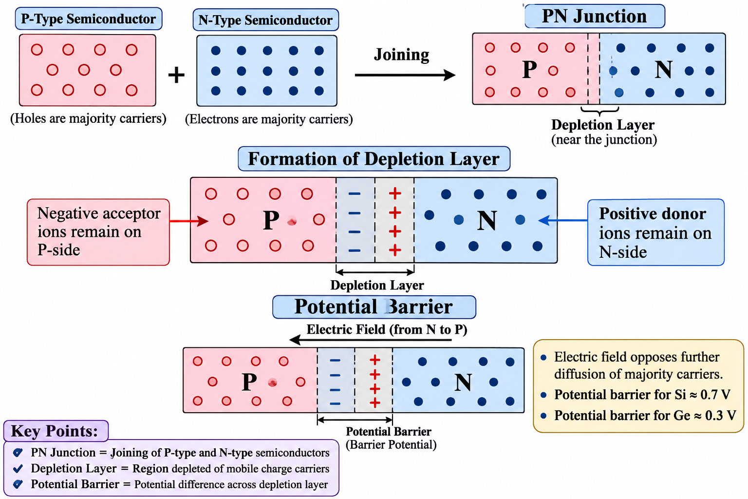
A PN junction is formed by joining a P-type semiconductor with an N-type semiconductor. When these two regions are joined, electrons from the N-region diffuse towards the P-region, while holes from the P-region diffuse towards the N-region. Near the junction, electrons and holes recombine, resulting in the formation of a depletion layer. Due to immobile ions, an electric field is developed across the depletion region, which produces a potential barrier.
Answer the following questions:
(a) What are the majority charge carriers in P-type and N-type semiconductors?
(i) Electrons and holes (ii) Holes and electrons (iii) Protons and electrons (iv) Neutrons and holes
(b) The depletion layer is formed due to:
(i) Drift of electrons only (ii) Recombination of electrons and holes (iii) Movement of protons (iv) Heating effect
(c) Which ions are present on the P-side of the depletion layer?
(i) Positive donor ions (ii) Negative acceptor ions (iii) Positive donor and negative donor ions (iv) Neutral ions
(d) The potential barrier for a silicon PN junction is approximately:
Case Study – 2: questions based on the forward and Reverse Biasing
A PN junction diode can be connected to an external battery in two ways: forward biasing and reverse biasing.
In forward biasing, the P-side is connected to the positive terminal and the N-side to the negative terminal of the battery. This reduces the depletion layer width and potential barrier, allowing current to flow easily.
In reverse biasing, the P-side is connected to the negative terminal and the N-side to the positive terminal. This increases the depletion layer width and potential barrier, resulting in a very small current.
Answer the following questions:
(a) In forward biasing, the P-side is connected to:
(i) Negative terminal (ii) Positive terminal (iii) Both terminals (iv) Ground
(b) During forward biasing, the depletion layer width:
(i) Increases (ii) Decreases (iii) Remains constant (iv) Becomes infinite
(c) During reverse biasing, the current through the diode is:
(i) Very large (ii) Zero in all practical conditions (iii) Very small (iv) Infinite
(d) In reverse biasing, the potential barrier:
(i) Decreases (ii) Increases (iii) Becomes zero (iv) Remains unchanged
Case Study – 3: Questions based on the semiconductor Diode as a Rectifier
A semiconductor diode is an important electronic device used for converting alternating current (AC) into direct current (DC). This process is called rectification.
A PN junction diode allows current to flow mainly in one direction. During the positive half-cycle of AC, the diode becomes forward biased and conducts current. During the negative half-cycle, it becomes reverse biased and does not conduct appreciable current.
Answer the following questions:
(a) The process of converting AC into DC is called:
(i) Amplification (ii) Rectification (iii) Modulation (iv) Oscillation
(b) A PN junction diode allows current to flow mainly:
(i) In both directions equally (ii) In one direction only (iii) In no direction (iv) Only in reverse bias
(c) During the positive half-cycle, a forward-biased diode:
(i) Does not conduct (ii) Conducts current (iii) Acts as an insulator (iv) Breaks down
(d) Which device is commonly used for rectification?
(i) Transistor (ii) Capacitor (iii) PN junction diode (iv) Resistor
Case Study – 4: Questions based on the Zener Diode****
A Zener diode is a specially designed semiconductor diode that operates in the reverse breakdown region. It is heavily doped and has a thin depletion layer. When the reverse voltage reaches a particular value called the Zener voltage, the diode starts conducting a large reverse current while maintaining an almost constant voltage across it. Therefore, it is commonly used as a voltage regulator.
Answer the following questions:
(a) A Zener diode is generally operated in:
(i) Forward bias (ii) Reverse breakdown region (iii) Zero bias (iv) Forward breakdown region
(b) A Zener diode is mainly used as:
(i) Current amplifier (ii) Voltage regulator (iii) Rectifier only (iv) Oscillator
(c) The depletion layer of a Zener diode is:
(i) Very thick (ii) Very thin (iii) Infinite (iv) Absent
(d) The voltage across a Zener diode in its breakdown region is approximately:
(i) Zero (ii) Constant (iii) Continuously increasing (iv) Infinite
Case Study – 5: Questions based on the Intrinsic and Extrinsic Semiconductors
Semiconductors are classified into intrinsic and extrinsic semiconductors. An intrinsic semiconductor is a pure semiconductor without any impurity. In an intrinsic semiconductor, the number of electrons is equal to the number of holes. When a small amount of impurity is added to a pure semiconductor, it becomes an extrinsic semiconductor. Depending upon the type of impurity added, it can be classified as P-type or N-type.
PN Junction Diode, Depletion Layer and Potential Barrier
Class 12 Physics – CBSE Board Examination
1. What is a PN Junction?
A PN junction is formed when a P-type semiconductor is joined with an N-type semiconductor in such a way that a continuous crystal structure is formed.
P-type semiconductor: It is formed by doping a pure semiconductor (Si or Ge) with a trivalent impurity such as Boron or Alluminium. Holes are the majority charge carriers.
N-type semiconductor: It is formed by doping a pure semiconductor with a pentavalent impurity such as Phosphorus or Arsenic. Electrons are the majority charge carriers.
When these two types of semiconductors are joined, a PN junction is formed.
2. Formation of Depletion Layer
The formation of the depletion layer in a PN junction takes place due to the diffusion of charge carriers.
Step-by-step explanation:
step-1; When P-type and N-type semiconductors are joined, there is a difference in the concentration of charge carriers on both sides.
step-2; Due to this concentration difference, electrons from the N-region start moving towards the P-region, while holes from the P-region start moving towards the N-region.
step-3; Near the junction, electrons and holes recombine with each other.
step-4; As a result of recombination, the region near the junction becomes free from mobile charge carriers.
step-5; The N-side near the junction develops positively charged immobile donor ions, whereas the P-side develops negatively charged immobile acceptor ions.
step-6; Thus, a thin region is formed around the junction which is depleted of free electrons and holes.
This region is called the depletion layer or depletion region.
Definition for CBSE Examination:
The region around a PN junction which is depleted of free electrons and holes due to the recombination of charge carriers is called the depletion layer.
Diagram of depletion layer:
3. What is Potential Barrier?
During the formation of the depletion layer, immobile positive ions are left on the N-side and immobile negative ions are left on the P-side.
These charged ions create an electric field across the depletion region.
This electric field opposes the further diffusion of majority charge carriers across the junction.
As a result, a potential difference is developed across the depletion layer.
This potential difference is called the potential barrier or barrier potential.
Definition for CBSE Examination:
The potential difference developed across the depletion layer of a PN junction, which opposes the further diffusion of majority charge carriers, is called the potential barrier.
Value of Potential Barrier
At room temperature (approximately 300 K):
Semiconductor
Potential Barrier
Silicon (Si)
0.7 V
Germanium (Ge)
0.3 V
4. How is the Depletion Layer Formed? (Complete Explanation)
The formation of the depletion layer can be understood through the following process:
As we know The P-region contains a large number of holes and N-region contains a large number of free electrons. After joining themElectrons diffuse from the N-region to the P-region Holes diffuse from the P-region to the N-region. Then the Electrons and holes recombine near the junction the mobile charge carriers disappear from this region.This is the cause of formation of immobile ions in which ,Positive donor ions remain on the N-side negative acceptor ions remain on the P-side. Finally, An electric field develops across the depletion region. A potential barrier is established. This barrier opposes further diffusion of majority charge carriers.
At equilibrium, the diffusion current and drift current become equal and opposite. Therefore, the net current through the junction becomes zero when no external voltage is applied.
5. Difference Between Depletion Layer and Potential Barrier
Depletion Layer
Potential Barrier
It is a region around the PN junction.
It is a potential difference across the depletion region.
It is formed due to recombination of electrons and holes.
It is developed due to immobile charged ions.
It contains immobile positive and negative ions.
It opposes the diffusion of majority charge carriers.
Its width can change with applied voltage.
Its value depends on the semiconductor material and applied conditions.
6. Important Questions for CBSE Board Examination
Very Short Answer Questions (1 Mark)
What is a PN junction?
Define depletion layer.
What is meant by potential barrier?
What are the majority charge carriers in P-type and N-type semiconductors?
What is the potential barrier of a silicon PN junction?
Short Answer Questions (2–3 Marks)
Explain the formation of a depletion layer in a PN junction.
What is potential barrier? How is it developed?
Why does the depletion layer contain immobile ions?
Why does the depletion layer oppose the flow of majority charge carriers?
Differentiate between depletion layer and potential barrier.
Long Answer Question (3–5 Marks)
Explain the formation of a PN junction with a neat labelled diagram. Describe the formation of the depletion layer and potential barrier.
Important Points to Remember for Students
PN junction = Joining of P-type and N-type semiconductors.
Depletion layer = Region depleted of mobile charge carriers.
Q.1. Show graphically how the energy emitted from a hot body varies with the wavelength of radiation. Give some of salient points of the graph.
Q.2. Explain why:
(a) a body with large reflectivity is a poor emitter.
(b) a brass tumbler feels much colder than a wooden tray on a chilly day.
.Q.3. Give four reasons why is mercury used in Thermometers
.Q.4. Give some merits of gas thermometers over those of mercury thermometers.
Q.5. Name the suitable thermometers to measure the following temperatures:(i) −80°C(ii) 60°C(iii) 250°C(iv)780°C(v) 2000°C
Q.7. What is meant by coefficient of linear expansion and coefficient of cubical expansion? Derive the
relationship between them.
Q.8. Two large holes are cut in a metal sheet. If the sheet is heated, how will the diameters of the holes change?
Q.9. In the above question (Q.8), will the distance between the two holes increase or decrease on heating?
Q.10. There are two spheres of the same radius and material at the same temperature, but one is solid while the other is hollow. Which sphere will expand more if:(i) They are heated to the same temperature.(ii) The same amount of heat is given to each of them.
Q.11. Two bodies of specific heats c1 and c2 , having same heat capacities are combined to form a single composite body. What is the specific heat of the composite body?
Q.12. Name the three modes of transfer of heat from one object to other. Also cite one example for each one of them.
Q.13. Define coefficient of thermal conductivity. Write its SI unit.
Q.14. Define thermal conduction and convection. How are these modes of transfer different from thermal radiation?
Q.15. Two rods A and B are of equal length. Each rod has its ends at temperatures T1 and T2 . What is the condition that will ensure equal rates of flow of heat through the rods A and B?
Q16. Distinguish between conduction, convection and radiation.
Q.17. Two vessels of different materials are identical in size and wall-thickness. They are filled with equal quantities of ice at 0°C. If the ice melts completely in 10 and 25 minutes respectively, compare the coefficients of thermal conductivity of the materials of the vessels.
Q.18. Two vessels A and B of different materials but having identical shape, size and wall- thickness are filled with ice and kept at the same place. Ice melts at the rate of 100 g min⁻¹ and 150 g min⁻¹ in A and B respectively. Assuming that heat enters the vessels through the walls only, calculate the ratio of thermal conductivities of their materials.
Q.19. Water in a closed tube is heated with one arm placed vertically above an arc lamp. Water will begin to circulate along the tube in a counterclockwise direction. Is this true or false?
Q.20. A sphere, a cube and a thin circular plate, all made of the same material and having the same mass, are initially heated to a temperature of 200°C. Which of these objects will cool fastest and which one slowest when left in air at room temperature? Give reasons.
.21. There are two rods of the same metal, same length, and same area of cross-section, but one of square cross-section and the other of circular cross-section. One end of each is kept immersed in steam. After the steady state is reached, the other ends of the rods are touched. Which one will be hotter? Give reason.
Q.22. Define Newton’s law of cooling. Write the expression.
Q.23. A solid sphere of copper of radius R and a hollow sphere of the same material of inner radius r and outer radius R are heated to the same temperature and allowed to cool in the same environment. Which of them starts cooling faster?
Q.24. On a hot day, a car is left in sunlight with all the windows closed. After some time, it is found that the inside of the car is considerably warmer than the air outside. Explain why.
q.25. How does tea in a thermos flask remain hot for long time?
Q.26. A blackened platinum wire , when gradually heated , first appears dull red then blue and finally white , explain why?
Q.27. In a coal fire, the pockets formed by coals appear brighter than the coals themselves. Is the temperature of such a pocket higher than the surface temperature of a glowing coal?
Define wave-front . What type of wave front will emerge from a point source and distance light source? Draw a wave front coming out from a (I)prism(II)concave and convex mirror(III)concave lens and(III)convex lens .
State Huygens principle, using this principle draw the diagram to show how a plane wave front incident(I) At the interface of two media gets refracted when it propagates from a rarer to denser medium, and hence verified Snell’s law and (II) At a plane surface and gets reflected and hence derive law of reflection.
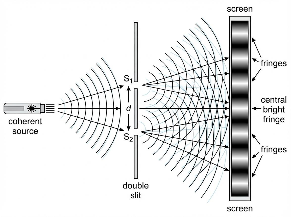
What are coherent sources of light ? Why two independent sources can’t be coherent ?why coherent sources are necessary to observing a sustained interference pattern ? How are the coherent sources are obtained in the Youngs double slit experiment?
What is interference of light? Write dawn the conditions to obtain the sustained interference fringe pattern. Show that the superposition of wave originating from two sources having displacement Y1 =a cosωt , Y2 =a cos(ωt+ɸ) at a point produces a resultant intensity ,I=4a2 cos2(ɸ/2) hence write the conditions for the appearance of dark and bright fringes.(* this question may be asked as deduce the conditions for constructive and destructive interference and hence write the expression for the distance between two consecutive bright or dark interference)
Using Youngs double slit experiment obtain the conditions for gating bright and dark fringes also derive the expression for the fringe width. Also write the effect on fringe width when(I)Distance between slits increases/decreases (II) Distance between slits and the screen increases/decreases(III) Monochromatic light replaced by white light,(IV) One of slit is closed and (V) entire experimental apparatus is immersed in a liquid
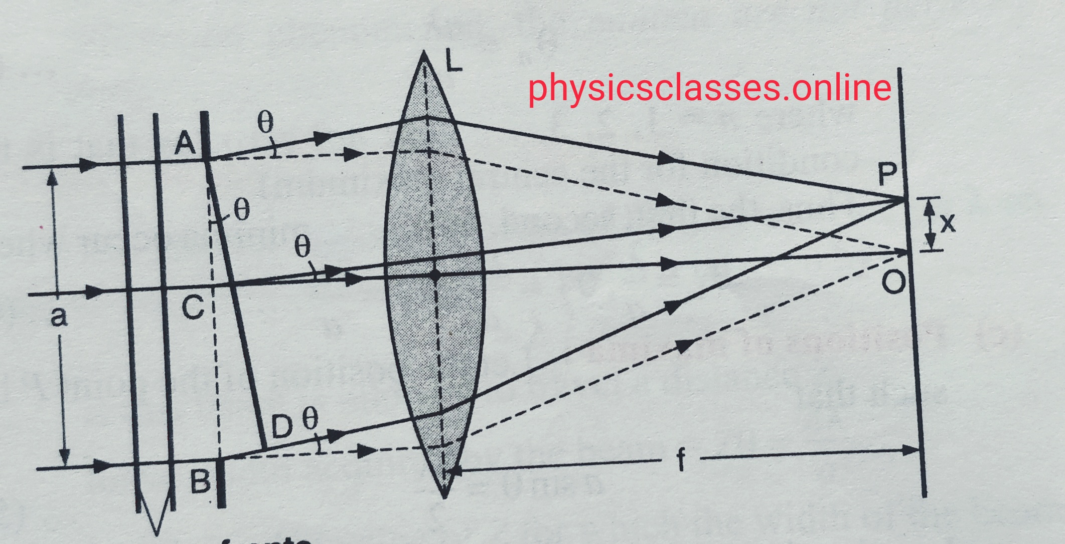
In a single slit diffraction experiment , deduce the conditions for the central maximum and secondary maxima/minima observed in diffraction pattern . Also explain why the secondary maxima go on becoming weaker in intensity as the order increases.(I) Haw does the width of the slit affected the size of the central bright fringe?(II)When a tiny circular obstacle is placed in the path of the light from a distant source , why is a bright spot seen at the centre of the shadow of the obstacle?(III) Show that the angular width of the central bright is two times the width of the first diffraction fringe (IV) If a mono chromatic source of light is replaced by white light , what change would you observe in the diffraction pattern?
In a modified setup of YDS experiment , it is given that SS2 – SS1 = λ/4 . (I) Obtain the condition for constructive and destructive interference at a point P on the screen in terms of the path difference მ = S2P -S1P . (II) Does the observed central bright fringe lie above or below O ? Give reason in support of your answer .
Before to solve this assignment , i want to inform that questions no. 7,8,9 and 10 is not in CBSE syllabus for board examination.
Important numerical of wave optics
1. In a Young’s double slits experiment fringes are obtained on a screen placed at certain distance away from the slits . If the screen is moved by 5 cm towards the slit , the fringe width changes by 30 μm . Given that the slits are 1mm apart . Calculate the wavelength of the light used . Ans- 600 nm.
2. Laser light of wavelength 640 nm incident on the pair of slits produces interference pattern in which bright fringe is separated by 7.2 mm . Calculate the wavelength of another source of light which produces interference fringes separated by 8.1 mm using same arrangement . Also find the minimum value of the order (n) of bright fringes of shorter wavelength which coincide with that of the longer wavelength . ans- 720nm , 9 .
4. Yellow light of wavelength λ= 6000 A illuminate a single slit of width 1 x 10⁻⁴ m calculate (i) the distance between two dark lines on either side of the central maximum when the diffraction pattern is on screen kept 1.5 m away from the slits , (ii) the angular spread of the first diffraction minima .
Ans- 1.8 cm , 6x 10⁻³ rad .
5. Two wavelength of sodium light 590 nm are used in turn , to study the diffraction taking place at the single slit of aperture 2x 10⁻⁴ m . The distance between the slits and the screen is 1.5 m . Calculate the separation between the position of first maxima of the diffraction pattern obtained in the two cases .
Ans-6.75×10⁻⁵m .
To watch the assignments of class 12th (cbse) click on the link given below-
6. (a) In a single slit diffraction , a slit of width d is illuminated by red light of wavelength 650 nm . For what value of d will (i) the first minimum fall at an angle of diffraction of 300 , and (ii) the first maximum fall at an angle of diffraction of 300 ?
(b) Why does the intensity of secondary maximum becomes less as compared to the central maximum .
Ans- 1.3 x10⁻⁶ m , 1.95×10 ‑6‑ m
7**. (i) Draw a graph showing the variation of intensity ‘I’ of polarised light transmitted by an analyser with angle ‘ϴ’ between polariser and analyser . (ii) What is the value of refractive index of a medium of polarising angle 600 . Ans- ip =600 , √3 .
8**. Two polaroids are set in crossed positions. A third polaroids is placed between the two making an angle ϴ with the pass axis of the first polaroid . Write the expression for the intensity of light transmitted from the second polaroid . In what orientations will the transmitted intensity be (i) minimum and (ii) maximum ?
Ans- 0 or ∏/2 ; 450
9**. Two polaroids P1 and P2 are setup so that their pass axis are crossed with respect to each other . A third polaroid P3 is now introduced between these two so that its pass axis makes an angle ϴwith the pass axis of P1 . A beam of unpolarised light of intensity I0 is incident on P1 . If the intensity of light that gets transmitted through the combination of three polaroids , be I find the ratio of I/I0 when ϴ equals (i) 300 (ii)450 . Ans- 3I0/32 ; 3/4
10**. Two polaroids P1 and P2 are setup so that their pass axis are crossed with respect to each other . A third polaroid P3 is now introduced between these two so that its pass axis makes an angle 300 with the pass axis of P1 . A beam of unpolarised light of intensity I0 is incident on P1 . If the intensity of light that gets transmitted through P1 ,P2 and P3 . Ans- I1=I0/2 I2 =3I0/8 , I3= 3I0/32
11. A monochromatic light of wavelength 500 nm is incident normally on a single slit of width 0.2 mm to produce a diffraction pattern . Find the angular width of the central maximum obtained on the screen . Also estimate the number of fringes obtained in YDSE with fringe width 0.5 mm , which can be accommodate within the region of total angular spread of the central maximum due to single slit . Ans- ϴ=0 to 2.5×10⁻³ ; n=D/2 ;D+1
12. A beam of light consisting of two wavelength 800nm and 600 nm is used to obtain the interference pattern in YDSE on a screen placed 1.4 m away . If the two slits are separated by 0.28mm , calculate the least distance from the central bright maximum where the bright fringes of the two wavelengths coincide .
13. In YDSE using monochromatic light of wavelength λ, the intensity of light at a point on the screen where path difference is λ is K units . Find out the intensity of light of light at a point where path- difference is λ/3 .
14. The ratio of the intensity at minima to the maxima in YDSE is 9:25 , find the ratio of the width of the two slits , also find the ratio of amplitude . Ans- 16:1 .
15. Two wavelength of sodium light of 590 nm and 596 nm are used in turn to study the diffraction taking place at a single slit of aperture 2×10⁻⁶ m . The distance between the slit and the screen is 1.5 m . Calculate separation between the position of first maxima and of the diffraction pattern obtained in the two cases .